")
")
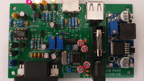 |
Our corsican repeater network TKNET uses the AllStarLink (ASL) software for the routing and communication between nodes needs a USB Radio Adapter (URA). In order to digitalize the audio signals and interface them with the repeaters, i developped a small interface board some years ago. It was using a cheap USB audio stick that we modified and plugged on my board. With time, this solution appeared to be not the best choice for different reasons. So, the idea to build a newer board with an onboard USB audio chip was born. Being retired, I found the time and mood to develop a new interface board using the same chip CM119A which is a small LQFP-48 case. |
Features :
- Onboard USB sound card compatible USB 2.0 and 48 kHz sampling rate.
- Powered via USB port or onboard stepdown regulator, jumper selectable
- Watchdog locking the PTT output in case of communication problem with the controler.
- 4 monitoring LEDs, Heardbeat, Squelch, PTT & OK.
- Left/right transmit audio channel jumper selectable
- Squelch level jumper selectable, ground or high level (open squelch)
- PTT output can be cut via jumper or switch (for tests, relaying OFF, etc...)
- 5 GPIO available, software programmable.
Connectivity :
- 2mm power Jack to power the onboard 5V/3A power supply (max 30V input)
- Port USB B for IN/OUT and connexion to computer or Raspberry board
- Port USB A to power an external board like a raspberry via a USB cable (USB C, etc...).
- DSUB- 9 female connector for RADIO inputs/outputs (PTT, SQ, AF TX & AF RX)
- GPIO4 to GPIO8 available on onboard pin connector.
Operation :
The board has its own power supply build around a small DC-DC buck converter that can power the interface and an external board (such as a RaspberryPi) via the USB A type connector. The input is max 30V and it can furnish 3A. The output is protected by a fuse F1.
A jumper can select the power source for the board the internal PS or via the USB A connector.
The heart of the interface is a CM119A chip that has a USB transceiver, voice DA + AD converters and 8 GPIO ports.
It has an oscillator with an external 12 MHz crystal.
The LED0 output on pin 12 drives the Led HB (heartbeat) that monitors the CM119A state. Blinking shows a USB dialog and steady that the chip is powered and waiting.
This LED0 output is also used to drive a Watchdog build around a NE555 triggerable astable. As soon as the LED0 stops blinking, the Watchdog puts the NE555 output in a LOW state. Transistor Q4 is not driven anymore and locks the PTT line via Q3 which is the PTT switch.
The Watchdog is preventing a steady carrier situation if the controler software crashes.
The PTT function is done via CM119A pin 13 GPIO3. Transistor Q3 drives the transmitter. The jumper JP4 can be used to interrupt the PTT line in removing this jumper and/or wiring a front panel switch.
The Squelch input drives transistor Q1 to pin 48 VOLDN and tells the software that a carrier is present.
Jumper JP2 allows 2 Squelch states :
WITHOUT : the receiver must provide a voltage when NO signal. Max. voltage is 5V, even if there is a 5V Zener protection on board.
WITH : the receiver must provide a close contact when NO signal. A 5V is then present on the input.
The right or left audio channel at CM119A outputs are selectable with jumper JP3 and driven to the transmitter via the RP1 variable resistor.
Resistor R7 in serial with RP1 can help to adjust the output level setting. Some transmitters do need a very low input level and the RP1 setting can be a little critical. R7 can be omitted in most cases and replaced by a wire jumper.
The AF signal from the receiver is driven to pin 27 MICIN via the RP2 variable resistor.
Building the board:
The printed board has been drawn with EASYEDA. PCBs have been ordered at their partner JLCPCB which i use regularly to my great satisfaction ! Recommended !
The big advantages of EASYEDA is that it doesn't need any installed software, is Web oriented so allows working from anywhere on this planet and with a team. (even if i did it alone..)
BOM bill of materials ODT format with MOUSER references. Some components were ordered via Aliexpress.
Component side of the board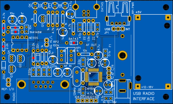
Solder side of the board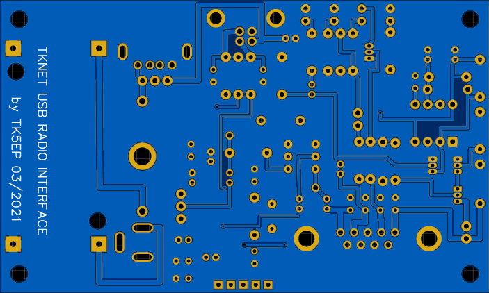
The most difficult task is to solder the CM119A which is a LQFP-48 case. But with a small soldering iron, a good view (i wear glasses), solder flux and a calm hand (i have one), the job can be done ! I did it at my age and bad close view ;-)
I double checked the continuity from the CM119A pins with the help of the schematic. Check solder bridge as well.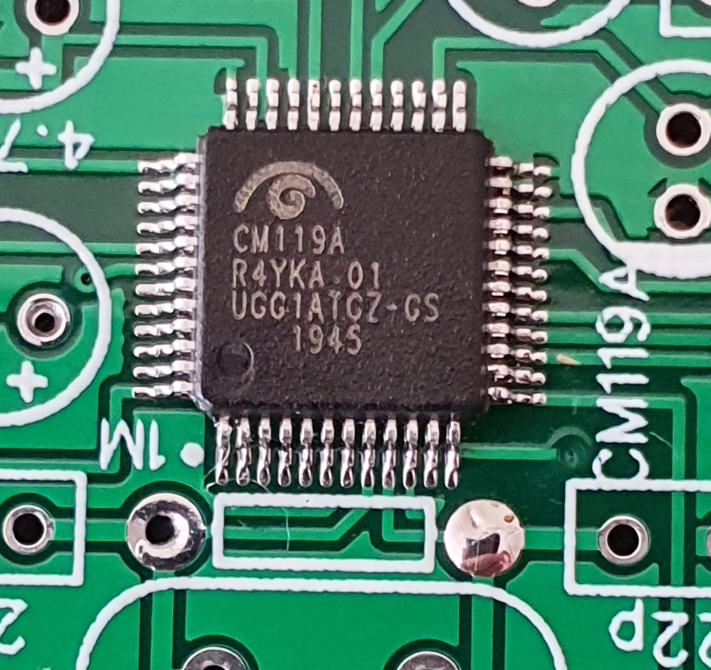
As often, the first version of a PCB has some errors, i didn't make an exception. I made 3 small silkscreen errors.
BEWARE, the diagram and picture in this article are the good one, the concerned parts are marked with a red dot on the component side view above.
Only the PCB made on version 03/2021 have these errors.
- R4,R9,R12,R17 470 Ohm for brighter LEDs an correct an error in R17
- Diode D2 1N4148 reverted
- Diode D1 BAT43 reverted
- Resistors R10 4.7k & R11 1M have been swapped (around NE555)
- R13 & R16 values are 2.2k not 10k
If the board is to be powered via the USB B connector and if the internal power supply is not used to power the board and an external controler board, like the Raspberry Pi, the following parts can be omitted :
- DC1 power connector
- DC-DC buck converter U1
- Fuse holder F1
- Jumper JP1 replaced by a wire jumper in USB position.
- USB1 connector
The rest of the wiring is correct and does not need comments. Only the value of resistor R7 in serial with RP1 (TX level) has to be changed in order to adjust the output level to your transmitter needs.
R7 forms a voltage divider with RP1 and allows to adjust the setting coarse. It can be replaced be a wire jumper in most cases.
C3 on the USB port supply is not mandatory and can be omitted if no problem. (i didn't have any)
BEFORE powering the board, inserting the fuse and jumper JP1, you must ABSOLUTELY set the output voltage of the DC-DC stepdown regulator LM2596 in order to have a precise 5V on the output ! Very often, the boards come with the variable resistor at full value and the board delivers >12V !!
Tests :
Make a loopback between the audio ouput and input in bridging pins 1 & 2 on the DSUB RADIO connector
Put jumper JP1 on the USB position in order to power the board via the USB port.
Connect the board to a computer with a USB A-B cable. The HB Led should light up showing that the board is powered and Windows should detect a new audio device "USB PnP audio device", as well as a new composite device.
At this stage, the HB Led should be steady and the OK Led OFF.
In the sound parameters, the new device should appear in both INPUT and OUTPUT device selection.
Select it in both.
The HB Led should blink and the OK Led should light, showing that the Watchdog is working fine.
Load and read a sound file and check if the level gauges are moving for both Input and Output.
Check that both levels are adjustable with the RP1 et RP2 adjustable resistors.
Unselect the new sound device, the OK Led shoud be OFF and the HB Led steady.
If everything is OK at this stage, congratualtions ! If not, start to check the board wiring... :-(
The JP2 jumper is modifying the Squelch operation :
Without jumper : the squelch signal from the receiver should provide a voltage when Squelch is unactive (5V max) and 0V when active.
With jumper : The squelch signal from the receiver must be an open collector and short with inactive Squelch
Test : Insert a jumper on JP2 , the SQ Led should light. Put the SQ input on DSUB RADIO pin 4 at ground, the LED should be OFF
The PTT line can be tested with a small utility found in the DireWolf package, namely CM108.EXE (release download page) which switches the GPIO3.
In a DOS CMD window, launched without parameters it lists all sound devices :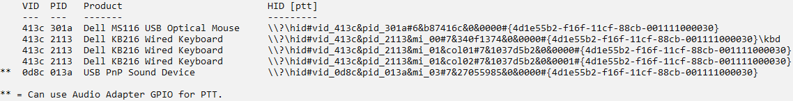
Copy the complete line with the HID number and launch the following line for the above example :
cm108 "\\?\hid#vid_0d8c&pid_013a&mi_03#7&27055985&0&0000#{4d1e55b2-f16f-11cf-88cb-001111000030}"
The PTT Led should blink at a 1s rate and the screen show a list of 10101010101. The PTT line (pin 5 on DB9) should also be activated on the same rate.
Commissionning :
Put a jumper on JP1. USB side if the board has to be powered via the USB port or INT side if the internal power supply i used.
Put a jumper on JP2 if the Squelch signal is a open collector output. (see details above)
Put a jumper on JP3 on L or R depending of the audio channel used in the controler.
Put a jumper on JP4 in no switch for relaying in not present on the front face. (see details above)
Connect the USB B cable to the PC or controler board.
Connect an external power supply on DC1, max 30V/3A. (if needed)
Launch the controler software. The HB Led should blink and the OK Led light ON. Check the good working and adjust the audio levels with help of the software and the RP1 & RP2 pots.
DSUB RADIO connector wiring :
- 1 - RX AF coming from receiver
- 2 - TX AF going to transmitter
- 4 - SQUELCH signal coming from receiver, 5V max or open collector.
- 5 - PTT signal to transmitter (open collector) 15 V max.
- 3+6+6+7+8 Ground
- 9 N.C